Technology
In future, world should hear ‘Digital India Inside’: MoS IT
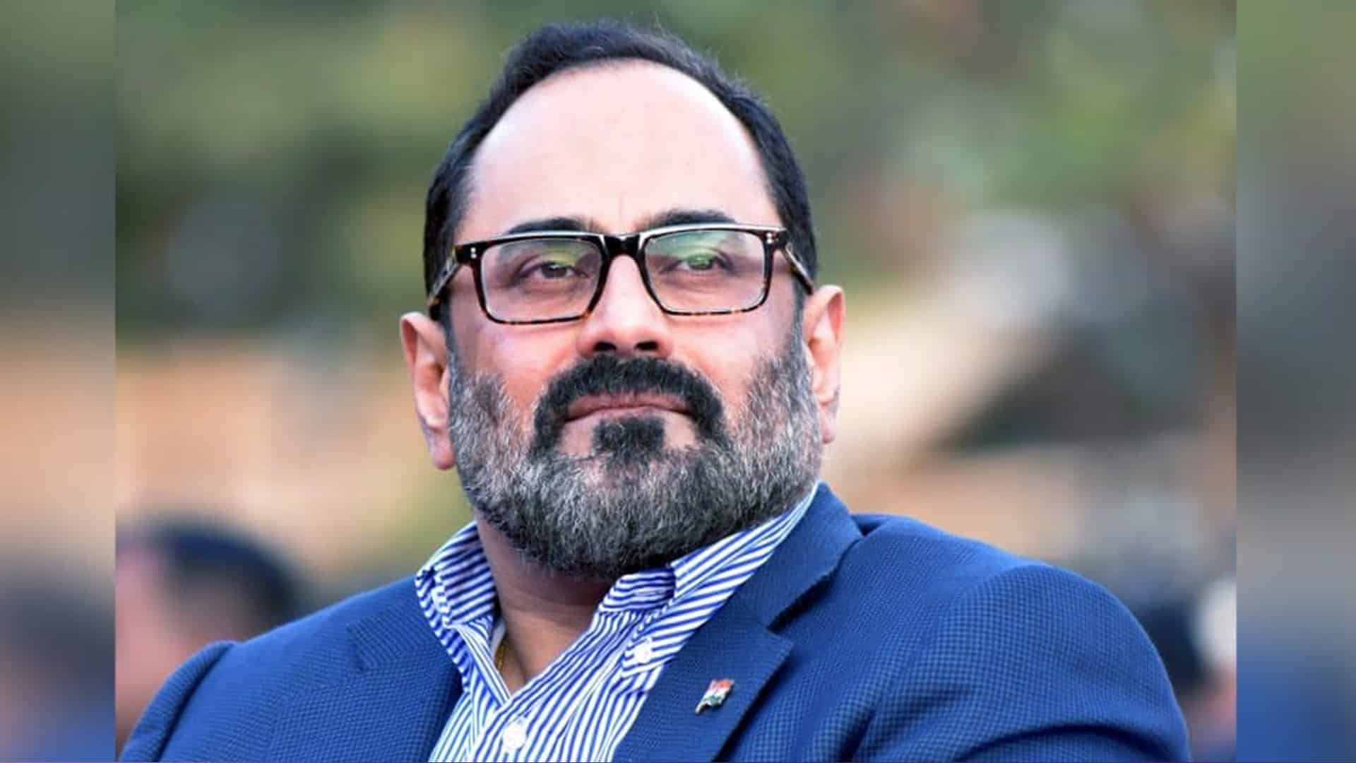
Giving the analogy of chip major Intel’s famous slogan “Intel Inside”, Minister of State for Communications and IT Rajeev Chandrasekhar on Sunday said all efforts of the government in the semiconductor domain should make the world hear “Digital India Inside”.
The minister also said industry players like Dell, Sony as well as ISRO and the Atomic Energy Department are all endorsing and working with the Digital India RISC-V (DIR-V) programme. The government has set a deadline to commercially launch the first indigenous chipset by 2023-24 under the DIR-V. “In the past, world heard Intel Inside. In the future, the world should hear Digital India Inside,” Chandrasekhar said.
Also read: Rising COVID cases early hints of 4th wave; will not impact growth in near-term: Nomura
He further said the government will review norms of the design linked incentive (DLI) program which envisages to support 100 companies involved in product design in the semiconductor space as part of the Rs 76,000 crore scheme for developing the electronic chip ecosystem in the country. The scheme will continue to be in place to support all product design projects and start-ups, among others, he added.
“Whether the DLI norms need to be modified… We have got some feedback from this conference that maybe the DLI has been designed to be very narrow. Maybe there is a cap on funding that is too restrictive. We will examine all that,” Chandrasekhar told reporters. He was addressing the media at the Semicon India 2022 conference after seven memorandums of understanding (MoUs) were signed between government organisations and technology companies.
“I want to say this very clearly that the USD 10 million package of the Rs 76,000 crore package is for the ecosystem and design and innovation is a very important part of the ecosystem. Talent is a very important part of the ecosystem. There is a need to sort of redesign some of those pieces, we will do it,” Chandrasekhar said.
The scheme provides for reimbursement of up to Rs 30 lakh per application for MPW (multi-project wafer) fabrication of design and post-silicon validation activities; reimbursement of up to 50 per cent of the eligible expenditure subject to a ceiling of Rs 15 crore per application for designing semiconductor goods; and reimbursement of 6 to 4 per cent of net sales of designed semiconductor goods over 5 years subject to a ceiling of Rs 30 crore.
At the event, the Ministry of Electronics and IT announced the onboarding of Prof Rao Tummala from Georgia Tech University, US, on the Advisory Committee of India Semiconductor Mission. MoUs were signed between Cyient, WiSig Networks and IIT Hyderabad to enable mass production of “5G Narrowband-IoT- the Koala Chip, Architected and Designed in India”.
Signalchip Innovations, Ministry of Electronics and IT (MeitY) and the Centre for Development of Advanced Computing (C-DAC) signed an agreement for not only design and manufacture but also deployment and maintenance of 10 lakh Integrated NavIC (Navigation with Indian Constellation) and GPS Receivers. State-run CDAC announced partnership with Synopsys, Cadence Design Systems, Siemens EDA and Silvaco for making available their Electronic Design Automation (EDA) tools and design solutions for Chips to Startup (C2S) Programme being implemented by CDAC.
Chips to Startup (C2S) Programme of MeitY aims to create 85,000 specialised engineers at B Tech, M Tech and PhD levels for expanding Indian semiconductor talent at over 100 institutions across the country. Besides, Semiconductor Research Corporation (SRC) USA and IIT Bombay will focus on bringing together SRC’s industry experts and India’s R&D talent to create an industry driven research and development program.


Pingback: India-UAE trade pact comes into force